Design for Manufacturability

Technology section

Our Suggested DFM Guidelines

We understand fine design features can be difficult to avoid with today’s technological demands. However, following these guidelines can help keep costs down and allow for smoother fabrication processes. Good design practice suggests only running close constraints when necessary.

View our complete manufacturing capabilities

Widths and Clearances

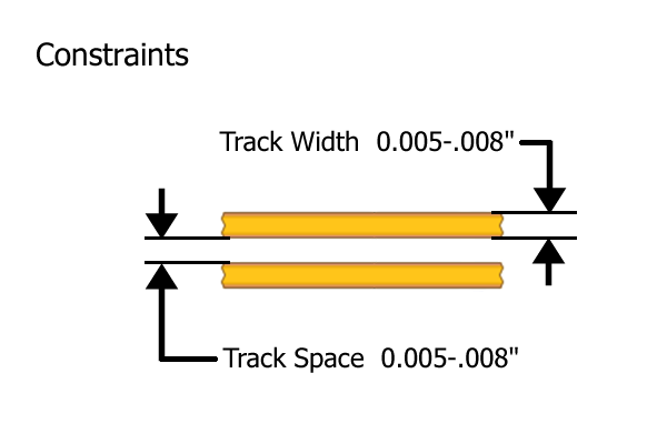
  • Wire rout tracks and buses at width of 0.005-.008″ (0.125-.20 mm).
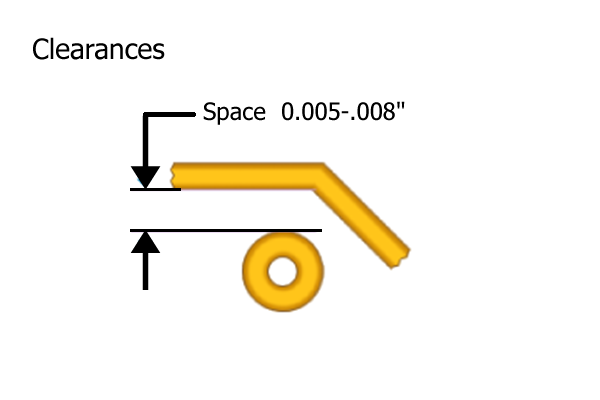
  • Keep copper clearances for trace-to-trace at 0.005-.008″ (0.125-.20 mm).
  • Copper-to-board-edge at 0.015-0.020″ (0.40-.50 mm).
  • Keep solderable component pads away from board edge, 0.20-.30″ (5.00-7.50 mm).
dfm_gap
dfm_tracks

Hole Types

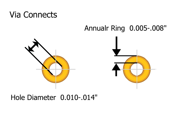
  • Vias diameters 0.010-.014″ (0.25-.35 mm) with 0.005-.008″ (0.125-.20 mm) annular ring each side.
  • Functional through-hole annular rings 0.010-.015″ (0.25-.40 mm) depending on the hole diameter.
  • Plated Slots, 0.026-.040″ (7.00-1.00 mm). A slots >0.040″ (1.00 mm) is typically routed instead of drilled.
  • Non-Functional (non-plated holes) are typically routed instead of drilled >0.250″ (6.35 mm).
dfm_vias

Soldermask and Silkscreen

  • Soldermask webbing/space between component pads at 0.004-.006″ (0.10-.20 mm).
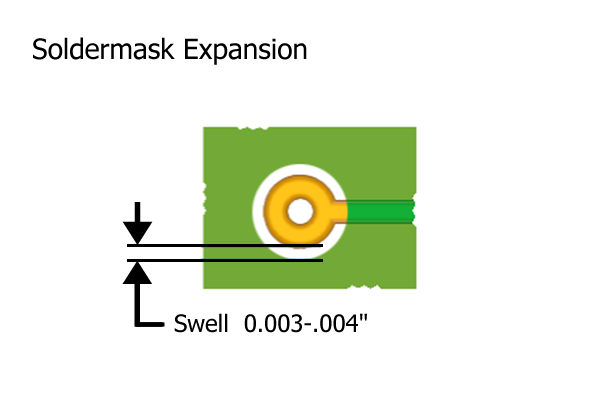
  • Soldermask swell at 0.003-.004″ (0.80-0.10 mm).
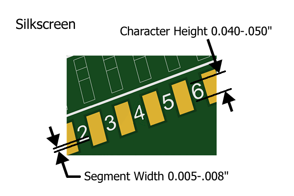
  • Silkscreen segment widths at 0.005-.008″ (0.125-.20 mm).
  • Silkscreen character height 0.040-.50″ (1.00-1.30 mm).
dfm_soldermask
dfm_silkscreen

Adding Teardrops

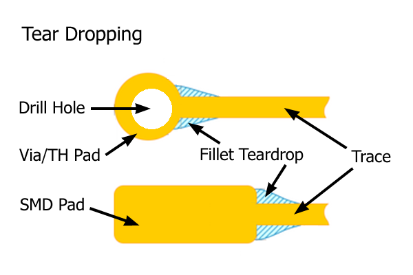
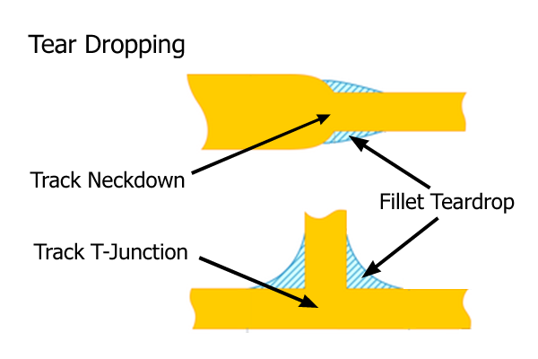
Teardrops can be added to the design to help prevent drill break-out and fill any corner angled track junctions. Standard deviation can allow some drill wander and layer registration during manufacturing. Adding teardrops to the though-hole pads can help prevent any drill break-out. We recommend adding on fine featured designs where the annular ring are below 5 mils (.005″).

Surface mount pads and track junctions can benefit from teardrops. Solution and chemistry can get trapped in sharp corner creating etching or adhesion issues during manufacturing. Sharp edge junctions can incur unwanted resistance creating heat and even damage the copper circuit depending on the current.

dfm_teardrop-pad
dfm_teardrop-track

Thieving

Thieving is used to balance copper distribution across the circuit layers. A non-conductive pattern is printed to the signal layers with clearances around functioning lands and circuits.

This can be added during the CAD board design level or during the front-end CAM pre-production steps.


Surface Pad Via Options

The three typical via options when designing your board are, ‘Dog Bone Via’, ‘Via with Pad Bump’, and ‘Via in Pad’.

  • Dog Bone Via: Most common and keeps the via hole away from the surface mount pad allowing for a good SMT placement without any additional manufacturing processes. Recommend covering or plugging via with soldermask to help prevent solder bridging.
  • Via with Pad Bump: Good option when board design has fine features with limited space. Via can be additionally plugged with via-fill compound but not necessary. Via fill process adds cost to the PCB.
  • Via in Pad: Used when limited design space and common with HDI designs. Via-fill with epoxy recommended to avoid solder wicking in the hole and potentially starving the surface pads during SMT. Can’t plug with solder resist.

Standard PC Board Thickness:

Thickness (in) Thickness (mm)
0.021"
0.50mm
0.031"
0.80mm
0.040"
1.00mm
0.062"
1.60mm
0.070"
1.80mm
0.093"
2.30mm

Copper Foil Weights / Thickness

Cu Weight (oz) Thickness (in) Thickness (mils)
1/4 (0.25)
0.00035″
0.35
1/8 (0.375)
0.00053″
0.35
1/2 (0.5)
0.0007″
0.7
1.0
0.00140″
1.4
2.0
0.00280″
2.8
3.0*
0.00420″
4.2
4.0*
0.00560″
5.6
6.0*
0.00840″
8.4
8.0*
0.01120″
11.2

* Considered heavy copper and may require a non-standard stackup. See our printed circuit board <stackup section> links to <stackup page> for more information.

Hint: As the copper increases in weight so should the copper-to-copper clearances. There is an etching factor which typically requires artwork to be swelled in order to achieve the design trace widths post etch and during layer inspection.

We review your CAD data prior to production to make certain it’s fit for fabrication.

If you need a second pair of eyes to review your design files, please send us the output files and we will run them through our front-end CAM system at no charge. For DFM review, we except data sets in Gerber, NC drill, and ODB++ data exports. Use our secure contact form to share files with our technical team in full non-disclosure.